
Description

Ball Grid Array (BGA) Packages and PCB Design Guidelines

PDF) Understanding and Improving Reliability for Wafer Level Chip
Introduction (Chapter 1) - Wireless Interface Technologies for 3D

15544557.ppt
Levels and Steps of Integration. Introduction, by Suny Li

2D, 2.1D, and 2.3D IC Integration

Materials, Free Full-Text

Figure 2 from Flip-Chip Technology on Organic Pin Grid Array

An efficient RDL routing for flip-chip designs - EDN
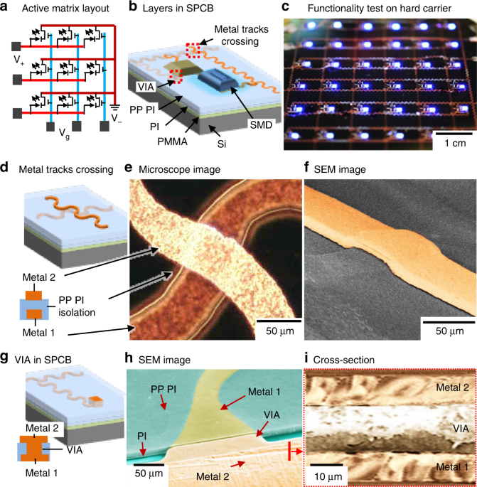
Integrated multilayer stretchable printed circuit boards paving

Hybrid Bonding Process Flow - Advanced Packaging Part 5
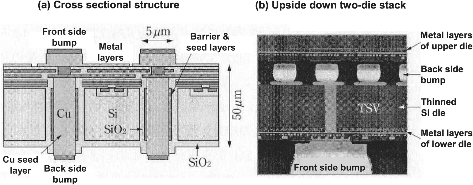
What Are Through-Silicon Vias?

Advanced Flip Chip Packaging
Related products


$ 24.99USD
Score 4.9(320)
In stock
Continue to book
$ 24.99USD
Score 4.9(320)
In stock
Continue to book
©2018-2024, belizeairportsauthority.com, Inc. or its affiliates